+86 134 0021 8776
+86 134 0021 8776
Mar. 02, 2023
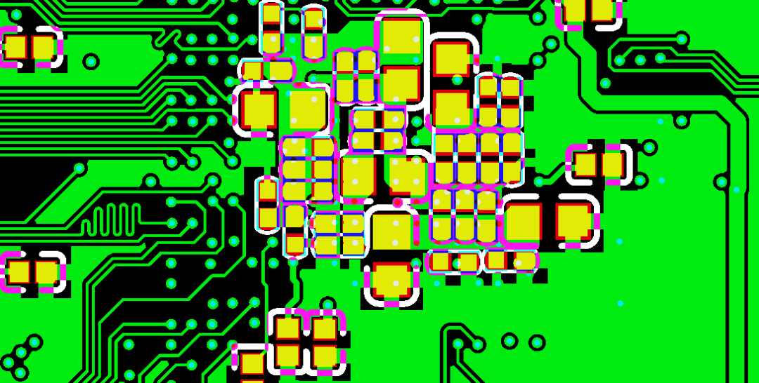
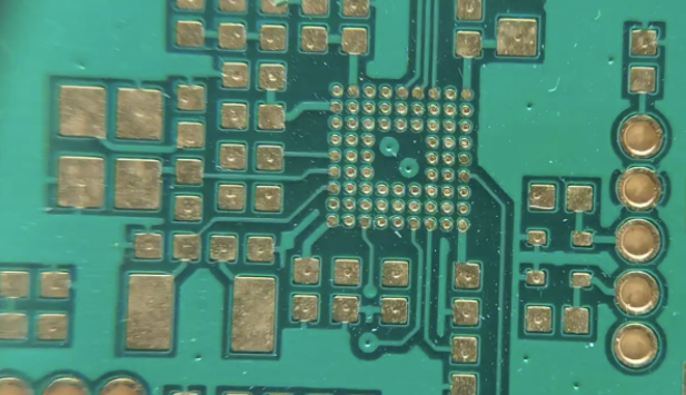
Via in pad on PCB is to the hole punched on the pad, the pad is SMD plate, usually refers to 0603 and above SMD and BGA pad, usually referred to as VIP(via in pad).The pad of plug-in hole cannot be called VIP, because the pad of plug-in hole needs to be welded with components, and all pin pads of plug-in have holes.
With the development of electronic products to light, thin, small direction, PCB board also pushed to high density, high difficulty development, so the volume of components is gradually getting smaller. For example, if the package of BGA components is small, the spacing of pins becomes smaller. If the pin spacing is small, it is difficult to wire the pins in the package, so it is necessary to change the layer and punch holes for wiring.
In BGA pin spacing is small, there is only one way to solve, which is via in pad. In addition, the filter capacitor is placed on the back of BGA. When there are many BGA pins, the filter capacitor on the back cannot avoid the hole out of the pin fan, and can only accept the hole on the pad of the filter capacitor. Therefore, there are two situations in the disk hole, one is on the BGA pad, the other is on the SMD pad.
The explanation of the hole on pad
1.via holes on the BGA
In general, there is no need to design VIP for packaging pins of devices, while many pins of BGA devices cause through holes to occupy wiring space. If through holes are designed as disk holes and holes are punched on BGA pads, wiring space can be reserved. When the spacing between pins is too small to wire, disk holes can be designed and routed from other layers.

2.The via holes on the filter capacitor
When many holes need to be punched in a BGA , it is difficult for the back-plug filter capacitor to avoid the holes. Therefore, the hole is punched on the pad and becomes the via in pad.

3.Do not do via-in-pad process on PCB board
The Via-in-pad requires a resin plug, which is then coated with copper to facilitate welding. When the resin plugging process is not done for Via-in-pad, the welding area will be small, and tin beads or oil explosion will occur in the hole, leading to virtual welding.

4.Do via-in-pad process on PCB board
BGA pad is small, such as redesign via-in-pad, basically no welding area. Therefore, the plate hole needs to be made of resin plug hole, electroplating to fill the hole is conducive to welding, there will be no bad welding phenomenon.

Therefore, it is recommended that in the case of sufficient spacing, try not to design via in pad, because the cost of manufacturing via in pad is very high and the production cycle is very long.
Previous: Solve the noise problem from PCB layout and wiring
Next: PCB packaging hole is small, component cannot be inserted, how to solve?
Hot Products
Navigation
+86 134 0021 8776
Floor 9, Aupu building, No. 395 XinShi North Road, Shijiazhuang Hebei, China
Request a Quote
