+86 134 0021 8776
+86 134 0021 8776
News
Mar. 24, 2023
The PCB is mainly composed of Copper Clad Laminates (CCL), semi-cured sheet (PP sheet), Copper Foil and Solder layer (also known as Solder Mask). At the same time, in order to protect the exposed copper foil surface and ensure the welding effect, PCB surface treatment is also needed, sometimes with characters for identification.
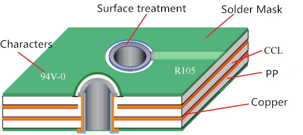
PCB 4 layers board structure diagram
1)Copper Clad Laminates (CCL)
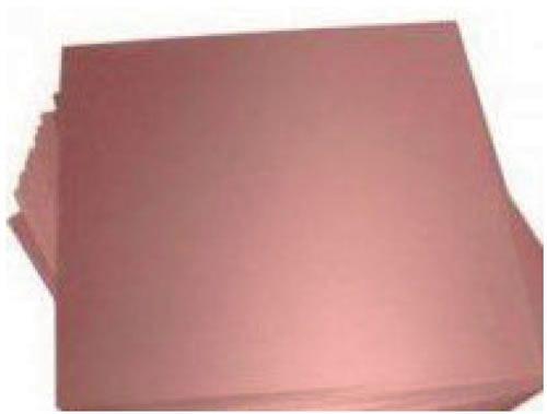
Copper clad laminate (CCL), referred to as copper clad laminate or copper clad laminate, is the basic material for manufacturing printed circuit boards. It is a composite material composed of dielectric layer (resin, glass fiber) and high purity conductor (copper foil).
At present, the most widely used PCB made by etching method is selectively etched on the copper board to obtain the required circuit pattern. Copper clad board in the whole printed circuit board mainly provides conductive insulation and support three aspects of the functions. The performance, quality and manufacturing cost of the printed circuit board depend largely on the copper-coated foil, as shown in Figure.
2)Semi-curing tablet
Semi-cured sheet, also known as PP sheet, is one of the main materials in the production of multilayer board. It is mainly composed of resin and reinforcement material. Reinforcement material is divided into glass fiber cloth (referred to as glass cloth), paper base and composite material.
Glass cloth is used as the reinforcing material for the semi-cured sheet (adhesive sheet) used in the manufacture of multi-layer printed circuit boards. The treated glass cloth is impregnated with resin glue, and then the thin sheet material is prebaked by heat treatment, which is called semi-cured sheet. The semi-cured sheet softens under heat and pressure and solidifies after cooling.
Due to the different number of yarn strands per unit length in the warp and weft direction of the glass cloth, it is necessary to pay attention to the warp and weft direction of the semi-cured piece during shearing. Generally, the warp direction (the direction of curling of the glass cloth) is selected as the short side direction of the production plate, and the weft direction is the long side direction of the production plate, so as to ensure the flat surface of the plate and prevent the distortion and deformation of the production plate after heating.
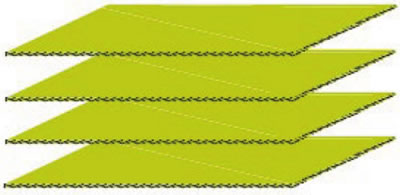
PP sheet
3)Copper
Copper foil is a thin layer of continuous metal foil deposited on the bottom layer of the circuit board. As the conductive body of PCB, it is easy to be bonded on the insulation layer, and the circuit pattern is formed after etching.
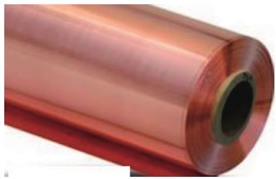
Common industrial copper foil can be divided into calendered copper foil (RA copper foil) and electrolytic copper foil (ED copper foil) two categories:
A.Calendered copper foil has good ductility and so on. It is the copper foil used in the early process of soft plate.
B.Electrolytic copper foil has the advantage of lower manufacturing cost than calendered copper foil, as shown in Figure.
4)Solder mask layer
Solder mask layer refers to the printed circuit board has solder resistance ink part.
Solder mask ink is usually green, a small number of red, black and blue, so in the PCB industry often referred to as the solder resistance ink green oil, it is a permanent protective layer of printed circuit board, can play the role of moisture-proof, anti-corrosion, anti-mildew and mechanical abrasion, but also can prevent parts from being welded to the wrong place.
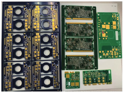
5)Surface treatment
Common PCB surface treatment processes include lead spray tin, lead-free spray tin, Organic Solderability Preservatives (OSP), gold deposition, silver deposition, tin deposition and gold-plated fingers. With the continuous improvement of environmental protection laws and regulations, lead preservatives have been gradually banned.
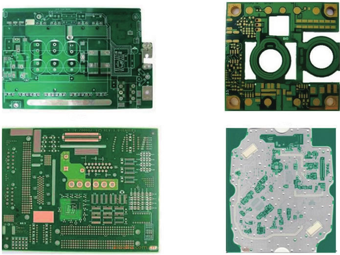
6) Characters
The character is the text layer, the top layer of the PCB, can not be, generally used for comments.
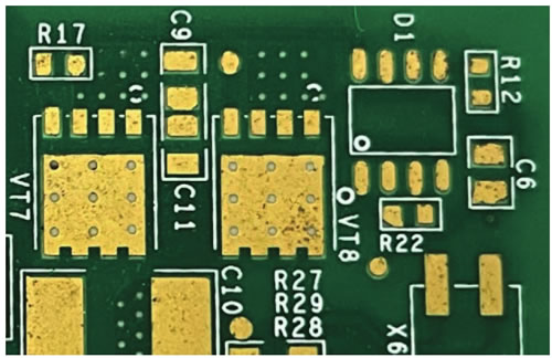
Usually, in order to facilitate the installation and maintenance of the circuit, the required logo pattern and text code are printed on the upper and lower surfaces of the printed board, such as the component label and nominal value, component outline shape and manufacturer's logo, production date, etc.
Characters are usually printed using screen printing, as shown in Figure.
Hot Products
Navigation
+86 134 0021 8776
Floor 9, Aupu building, No. 395 XinShi North Road, Shijiazhuang Hebei, China
Request a Quote
