+86 134 0021 8776
+86 134 0021 8776
Jul. 24, 2023
Gerber generated by protel is uniform and standardized, which is manifested in the following aspects:
1. The first g of the extension generally means gerber
2. The second extension represents the surface of the layer, b represents the bottom surface, t represents the top surface, g+ digit represents the intermediate line layer, g+p+ digit represents the power layer.
3. The last digit of the extension represents the class of the layer. l is the line layer, o is the screen printing layer, s is the solder resistance layer, p represents the solder paste, m represents the outer frame, reference hole, mechanical hole, other generally not important。
File extension:
Top (copper) Layer : ...........................................GTL
Bottom (copper) Layer :....................................... .GBL
Mid Layer 1, 2, ... , 30 : ...............G1, .G2, ... . .G30
Internal Plane Layer 1, 2, ... , 16 : ......GP1, .GP2, ... . .GP16
Top Overlay :............................................. .GTO
Bottom Overlay : ...........................................GBO
Top Paste Mask : ...........................................GTP
Bottom Paste Mask :....................................... .GBP
Top Solder Mask : ..........................................GTS
Bottom Solder Mask :...................................... .GBS
Keep-Out Layer : .........................................GKO
Mechanical Layer 1, 2, ... , 16 : ..........GM1, .GM2, ... , .GM16
Top Pad Master : .........................................GPT
Bottom Pad Master : ......................................GPB
Drill Drawing, Top Layer - Bottom Layer (Through Hole) : ...GD1
Drill Drawing, other Drill (Layer) Pairs : ...................GD2, .GD3
Drill Guide, Top Layer - Bottom Layer (Through Hole) : ...GG1
Drill Guide, other Drill (Layer) Pairs : .............GG2, .........GG3
Mechanical layer: defines the appearance of the entire PCB board, in fact, when we say the mechanical layer, we refer to the outline structure of the entire PCB board.
Prohibited wiring layer: define the boundary of the copper moment of our electrical characteristics in the cloth, that is, after we define the prohibited wiring layer, we will not exceed the boundary of the electrical characteristics of the cloth in the future cloth process.
Top overlay and bottom overlay: Define the top and bottom silk screen characters, which are the component numbers and some characters that we generally see on the PCB board.
Top paste and bottom paste: The top bottom pad layer refers to the exposed copper platinum that we can see. For example, we draw a wire on the top wiring layer. What we see on the PCB is just a wire, which is covered by the whole green oil, but we draw a square or a point on the top paste layer on the position of the line. This square and this point on the plate that you're punching out there is no green oil, it's copper platinum.
Top solder and bottom solder these two layers are just the opposite of the first two layers, it can be said that these two layers are to cover the green oil layer, multi-layer this layer is actually almost the mechanical layer, as the name means, this layer refers to all the layers of the PCB board.
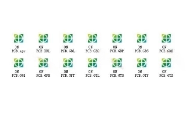
Attached to the generated Gerber file:

Hot Products
Navigation
+86 134 0021 8776
Floor 9, Aupu building, No. 395 XinShi North Road, Shijiazhuang Hebei, China
Request a Quote
